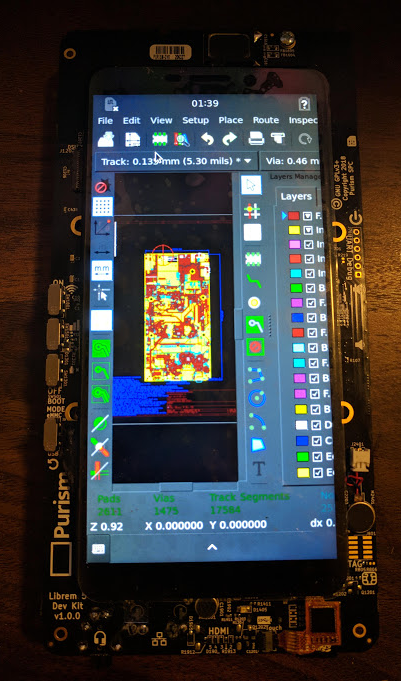
Librem 5 Dev Kit’s PCB layout viewed on the Dev Kit itself
Today we’re going to cover the journey of designing the Librem 5 Developer Kit and how 100% Free Software was used in its development.
The dev kit’s design is released under the terms of the GNU GPLv3+, its hardware Git repository can be found here: https://source.puri.sm/Librem5/dvk-mx8m-bsb
A backup mirror repo can be found here: https://github.com/gralco/dvk-mx8m-bsb
KiCad as The Obvious EDA of Choice
Before the development of the dev kit began, it was not completely clear which path we would take to produce the design, specifically, which Electronic Design Automation (EDA) tool would be used. Initially, the idea was to modify FEDEVEL’s i.MX 6QP OpenRex board, which would have satisfied the dev kit’s basic requirements, but we quickly met two major issues: it used the archaic i.MX 6QP, and even worse was that it was designed in the proprietary EDA suite Altium. Luckily, I had prior experience designing electronics using the EDA tool KiCad, so Purism had the opportunity to create a dev kit design which used 100% Free Software. KiCad was also an obvious choice not only due to its freedom-respecting license (GNU GPLv3+), but also because it is a very capable electronics design suite that even outperforms several pricey proprietary tools out there.
Selecting Components Which Met The Requirements
The first step when designing the dev kit involved searching for components that met the requirements which were defined in the Librem 5 campaign. In addition to meeting the specs outlined in the campaign, while searching for components, we decided to add quite a few extra bells and whistles; including:
- a lithium-ion charge controller (BQ25896)
- 18650 battery holder for an optional li-ion battery
- USB-C
- mini-HDMI
- SD card controller & micro-SD slot (since the i.MX 8M only has two uSDHC controllers)
- ethernet/RJ45
- audio codec
- earpiece speaker
- microphone
- CTIA/AHJ 4-pole 3.5mm headphone jack (with selection between on-board and external mic)
- GPG smart card reader & slot
- haptic/vibration motor
- user/software-controllable LED
- volume & power buttons
- hardware kill switches & boot-mode switch
- 16Mb SPI NOR flash
- a real-time clock (RTC)
We also added the to-be-expected through-holes for a UART debug header which is unpopulated by default (serial over USB works on the default image shipped with your dev kit). Hint: If you are not comfortable with a soldering iron then you may be able to use a press-fit header on these through-holes, search for the part-number Autosplice 23-1063. We included an SMD 2×5 JTAG footprint on the board and verified its functionality during the prototype phase; if this is something you’re interested in playing around with then have a look for the part-number GRPB052VWQS-RC.
For the WWAN/baseband modem and the Wi-Fi + BT we knew we needed to go with some sort of modules, surface-mount or otherwise. Early on, Nicole had the brilliant idea of using mPCIe and M.2 modules so as to make the dev kits modular and future-proof. We eventually nailed it down to the mPCIe SIMCom SIM7100A/E baseband modem module and the M.2 RedPine RS9116 Wi-Fi+BT module.
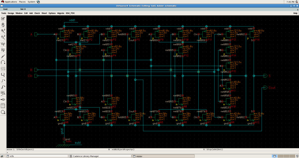
Beginning the Schematic Drawing
Initially, when the research phase was effectively over and we had to begin bringing our ideas into life, the i.MX 8M Quad had just recently become available on the market. In order to get a head-start in the development, add some extra modularity and future-proofness, we decided to go with a System-On-Module (SOM), which includes the SoC, SDRAM, eMMC, and PMIC. However, even in the early stages of the development when we began drawing the schematics, there were SOMs we were interested in that still didn’t get to their first production run. At around mid-April we established a natural relationship with EmCraft who were just getting into their first big SOM production run and were close to releasing its Hardware Architecture spec sheet. We determined that EmCraft’s SOM and their general resources were exactly what we needed. Once the specific SOM we were going to use was nailed down we were able to really begin cranking through the design.
The process of defining the specific components to be used on the dev kits was done concurrently while drawing the schematics. The entirety of the design was done using Git as our revision control system.
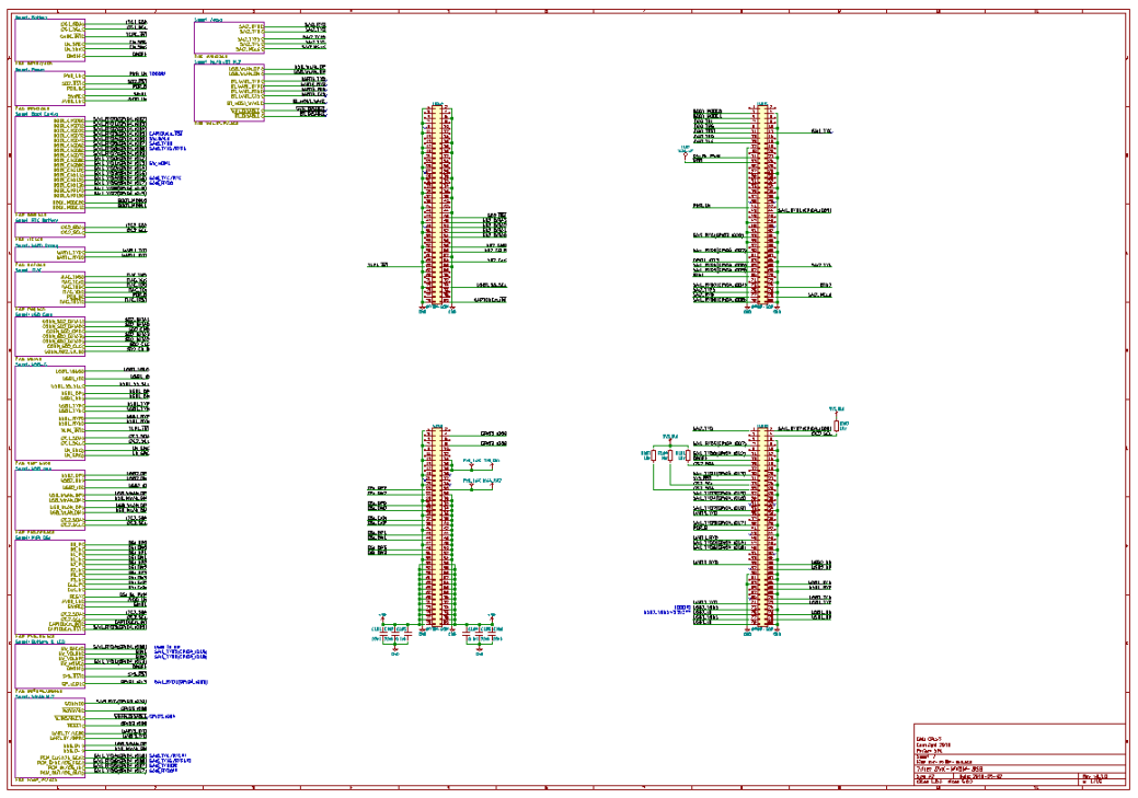 Figure 1: An early revision of the dev kit’s schematics from May 2nd (Git commit hash 023915d5)
After the schematic drawing was completed, we then exported our netlist file, getting us that much closer to the physical implementation of the dev kit.
HP_DET Simulation
In addition to using KiCad for the design of the dev kit, we also used a free software tool called Qucs-S and the free software SPICE-compatible simulation kernel called Xyce to simulate our headphone detect circuit, which included a zener diode used to protect the respective GPIO from too high or too low of input voltage from the audio codec’s HP DAC output. The combination of Qucs-S and Xyce allowed us to use the MMSZ4688T1G diode’s SPICE model in a circuit that best represented the physical conditions of nothing being inserted into the 3.5mm jack but the HP DAC output being active.
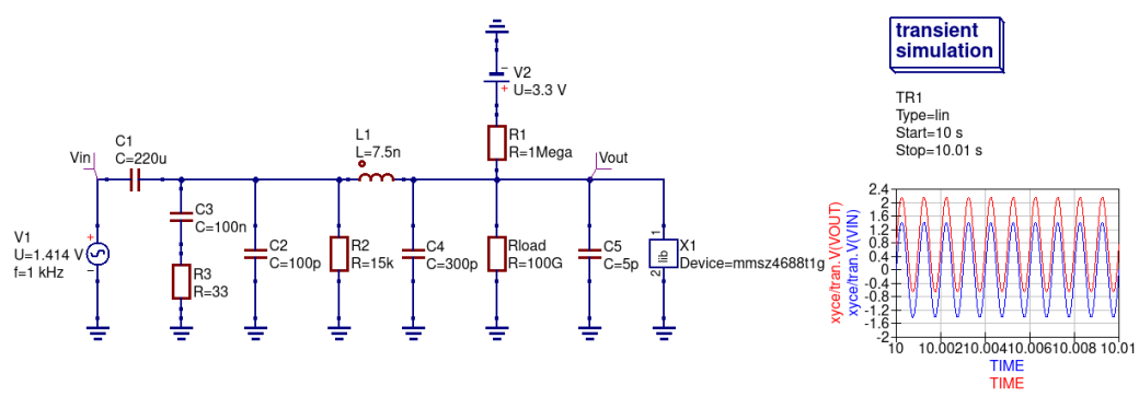 Figure 2: Qucs-S + Xyce simulation of the HP_DET circuit
This simulation, as well as the simple DC case where the 3.5mm jack’s internal switch is open and only the 1MΩ pull-up to 3V3_P, the optional internal pull-up, and the zerner are present, allowed us to prove that this protection method would work.
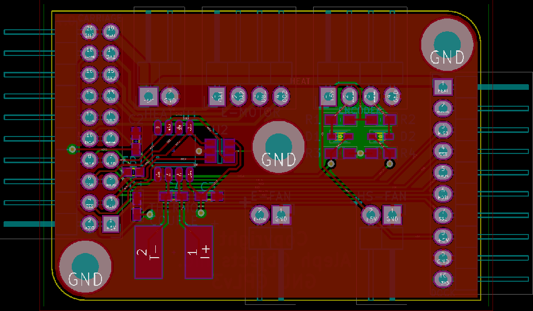
Creating Footprints
Around mid-June, when the Bill-Of-Materials (BOM) was complete and we began placing orders for the components, we were generating footprints for everything (chips, connectors, modules, etc). The process of creating these footprints involved going through each IC’s recommended land pattern as defined in their datasheet and quadruple checking to make sure everything was correct.
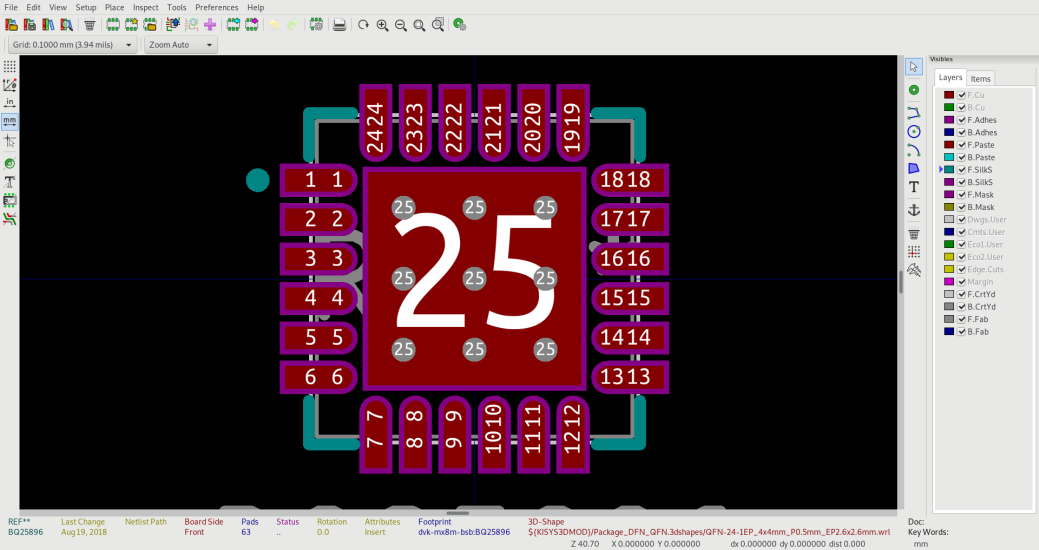 Figure 3: BQ25896 charge controller’s footprint (U301 on the dev kit board, found underneath the SOM)
Using KiCad’s amazing 3D viewer, we were able to give nearly every component a 3D model so as to help establish a tangible visualizer for the progress being made.
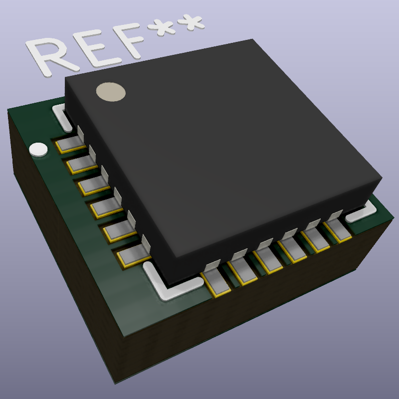 Figure 4: BQ25896 charge controller’s 3D view
Beginning Floorplanning, Routing, and Updating KiCad
Early on, a rough floorplan was made to help us establish how much board area was needed (90x180mm) and where the various larger components would go (connectors, receptacles, card slots, mPCIe & M.2 sockets, modules, etc). After really getting into the layout, some things continued to move around but were quickly pinned down on their specific locations.
In late-June we began routing, starting with the USB-C receptacle (commit a1bfc689). This marked the beginning of our layout process.
 Figure 5: First commit with routing involved
 Figure 6: What the USB-C routing eventually became
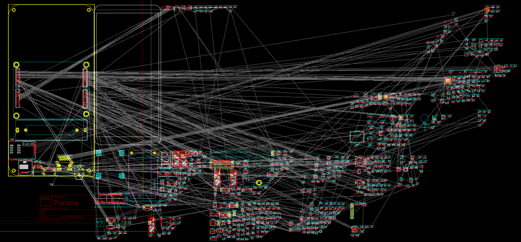 Figure 7: Early rats nest before component placement & routing
The routing process involved a delicate balance between working as quickly as possible while making sure everything done properly without error, including carefully routing controlled-impedance tracks and sensitive analog lines.
Initially we were unsure how many layers were needed and whether we needed components on both sides of the board. We knew that EmCraft’s i.MX 8M baseboard used 8-layers and had components on both sides, but we were pretty confident that we could at least cut down on the number of layers. We quickly realized that since we were going to have some components on the “back” of our board (display side), including the display connectors, proximity/ambient light sensor, user LED, speaker, and microphone, there would certainly be components on both sides of the board. Having components on both sides made the layout process somewhat easier since this freed up some space for where we could place the SPI NOR flash, smart card reader, RTC, 2.8V LDO, various ICs, passives, and other components. As for the number of layers, we decided to cut it down to 6-layers and would only add 2 additional layers if we were to hit a gridlock and not be able to route some nets; luckily this never happened and we were able to stick with just 6.
We opted to use a common stack-up which provides the best balance between ease of routing and reduces unintentional radiated emissions. The dielectric substrate that was used was NAN YA’s NP-180TL copper clad laminate, which has a relative permittivity of ~4.11 at our average operating frequency of ~1.7GHz. Our RF feedline calculations for the board’s microstrip and coplanar waveguide (CPW) feedlines using this stackup can be found in the Git repo.
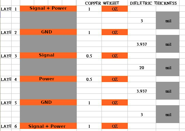 Figure 8: Dev kit stack-up
Before we began implementing the dev kit in KiCad we were not too sure if we wanted to use the nightly builds or stick with the somewhat older 4.0.7 stable release. Even though the nightly builds had several desirable features, we decided to go with the stable release so as to not have to frequently update KiCad and risk being on different versions. After getting a small dent into our layout, KiCad 5.0.0 was released! On July 16th we managed to update the dev kit project to KiCad 5.0.0 (specifically commits 4f70b865 and a4e3de8a) without much hiccup. Luckily, this update coincided with our switch from most passive components being 0603 to being 0402, since KiCad’s new passive footprints are a bit different than the old default ones, the pads having rounded corners which is more effective for lead-free solder.
After updating the project to 5.0.0 we were able to focus heavily on getting through the layout and were able to get the unrouted net count down to 0 within a month (August 14th, specifically commit 9b4dd2e0).
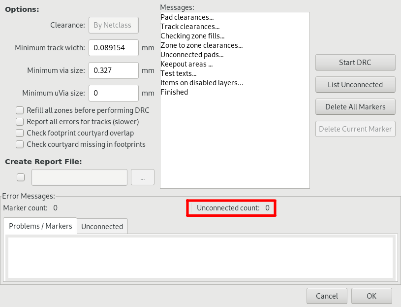 Figure 9: DRC on August 14th commit 9b4dd2e0 showing no unrouted nets and everything passing
When all nets were routed and the Design Rules Check (DRC) was passing, we were able to go back and tidy everything up for the next week or so.
Our most useful resources when laying out the board were the ICs’ layout reference found in either their datasheet or their evaluation board and Toradex’s Layout Design Guide which can be found here: https://docs.toradex.com/102492-layout-design-guide.pdf
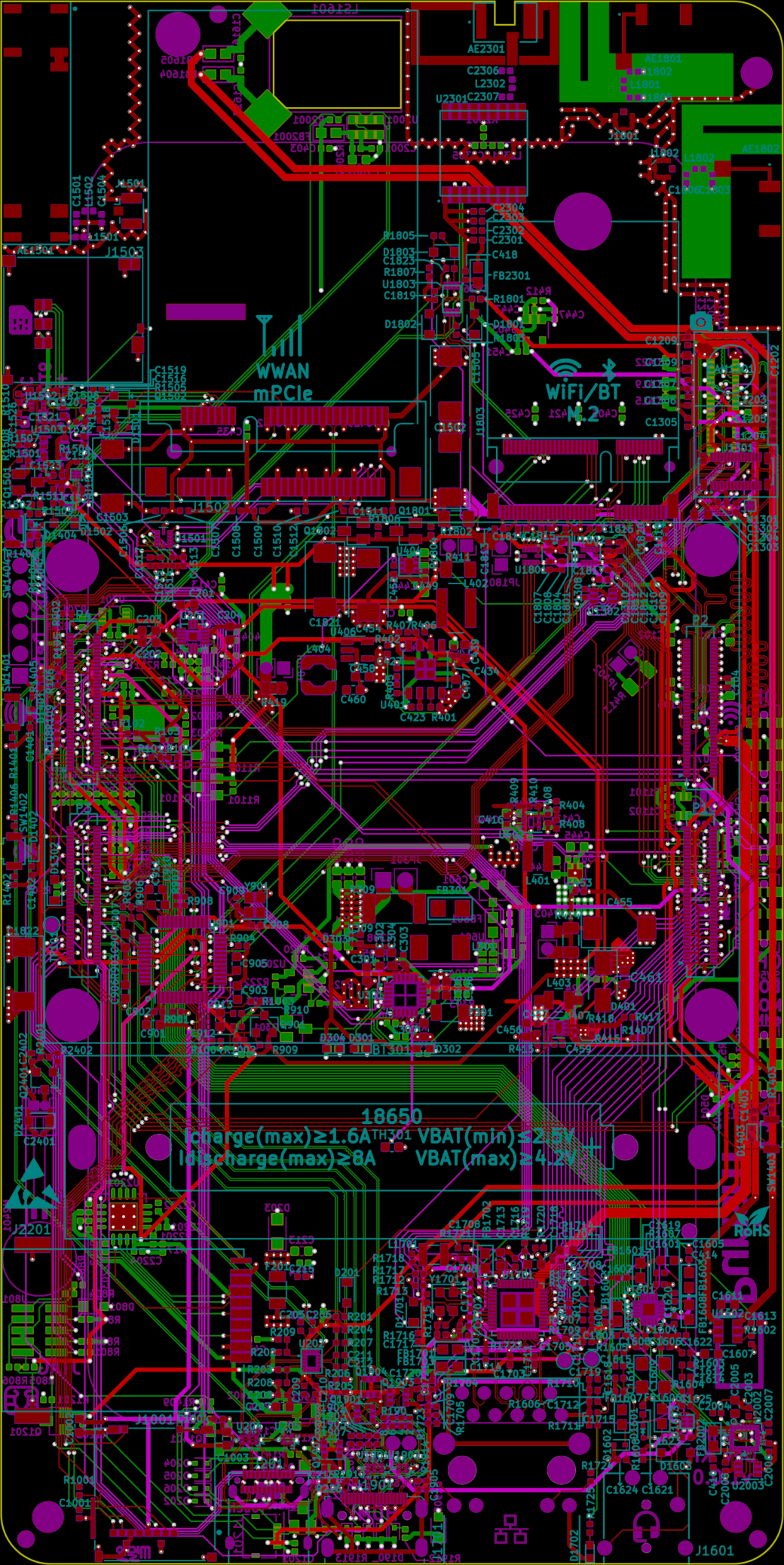 Figure 10: The final state of the layout (copper filled zones hidden)
Exporting Manufacturing Files and Sending Them Off For Fabrication
After the layout was considered complete, we had to export all of the necessary manufacturing files used to fabricate and assemble the boards. Exporting the Gerber files was straightforward since KiCad makes this step quite easy. However, our assembly house requested that we also provide a fabrication and assembly drawing which took more involvement to produce.
We mostly used gEDA’s Gerbv to preview our design’s exported Gerber files. A neat web tool that uses Gerbv and ImageMagick as its renderer is Gerblook, here’s a static link to the dev kits in Gerblook: http://gerblook.org/pcb/rTgd4Aqusxr7XQLSdKa9V3
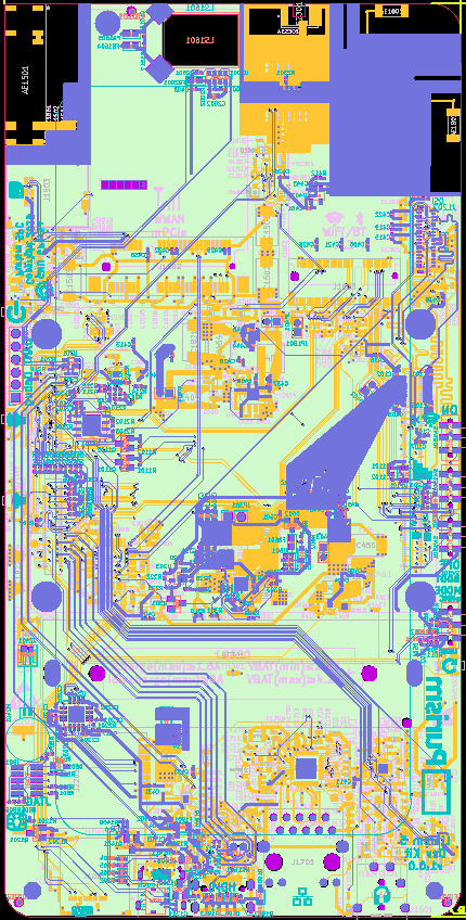 Figure 11: Dev kit’s Gerbers as viewed in Gerbv
In order to generate a proper assembly drawing, we made use of KiCad’s F.Fab/B.Fab layers to show the locations, outlines, polarity, and reference designators of all components on the board. By using each of the footprints’ F/B.Fab layers we were able to generate the final drawing by printing F.Fab and B.Fab onto separate PDFs and combining them afterwards.
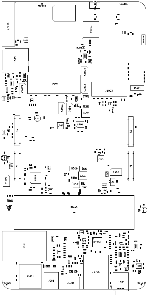 Figure 12: SOM side of the assembly drawing
The fabrication drawing was even more involved. To produce this, we needed to export the fabrication notes found on the Cmts.User layer along with the board’s outline as one DXF file and then export all of the drill marks as another DXF file. After these two files are generated, they are then combined and adjusted inside a footprint drawing. Then, once we have this special “footprint” that combines the two DXF files, we hide just about everything in the layout and import this special “fab” footprint (without saving this temporary layout). At this point, everything we need is found on the Dwgs.User layer; so we are able to print this along with the frame reference onto a final fabrication drawing PDF.
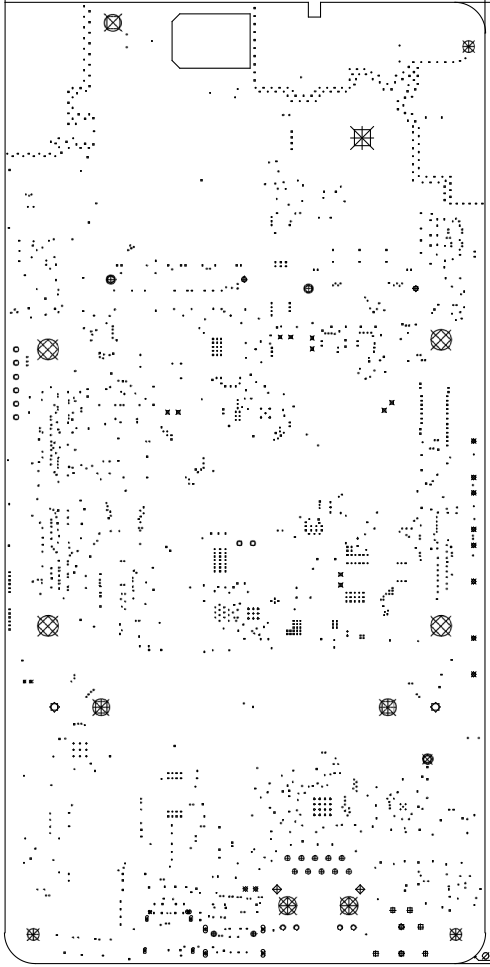 Figure 13: Drill markings in the fabrication drawing
Each of these files and documents are used along with the IPC-D-356 netlist (which allows the fabrication house to do a flying probe test on the boards to make sure there are no short/open circuits), a component placement list CSV file (for the assembly house to know where and what orientation all components are placed), and finally a manually-edited GenCAD file (which is used by the assembly house to program their solder paste machines for our board).
Testing Prototypes
After all of the final manufacturing files were delivered to the fabrication and assembly firms, we answered any questions they may have had during the process, and tweaked anything that may need to be adjusted based on their feedback. At around late August, the files were sent off and we were anxiously waiting for our design to hit the fabrication floor in Shenzhen. Unfortunately, as outlined in an earlier blog post, several unforeseen circumstances such as severe weather and most of China observing Golden Week, we saw significant delays in the production of our prototypes. Due to these delays, we decided to switch to a domestic factory for the fabrication of our prototypes, which managed to get the boards to us two weeks faster than the ones being made overseas.
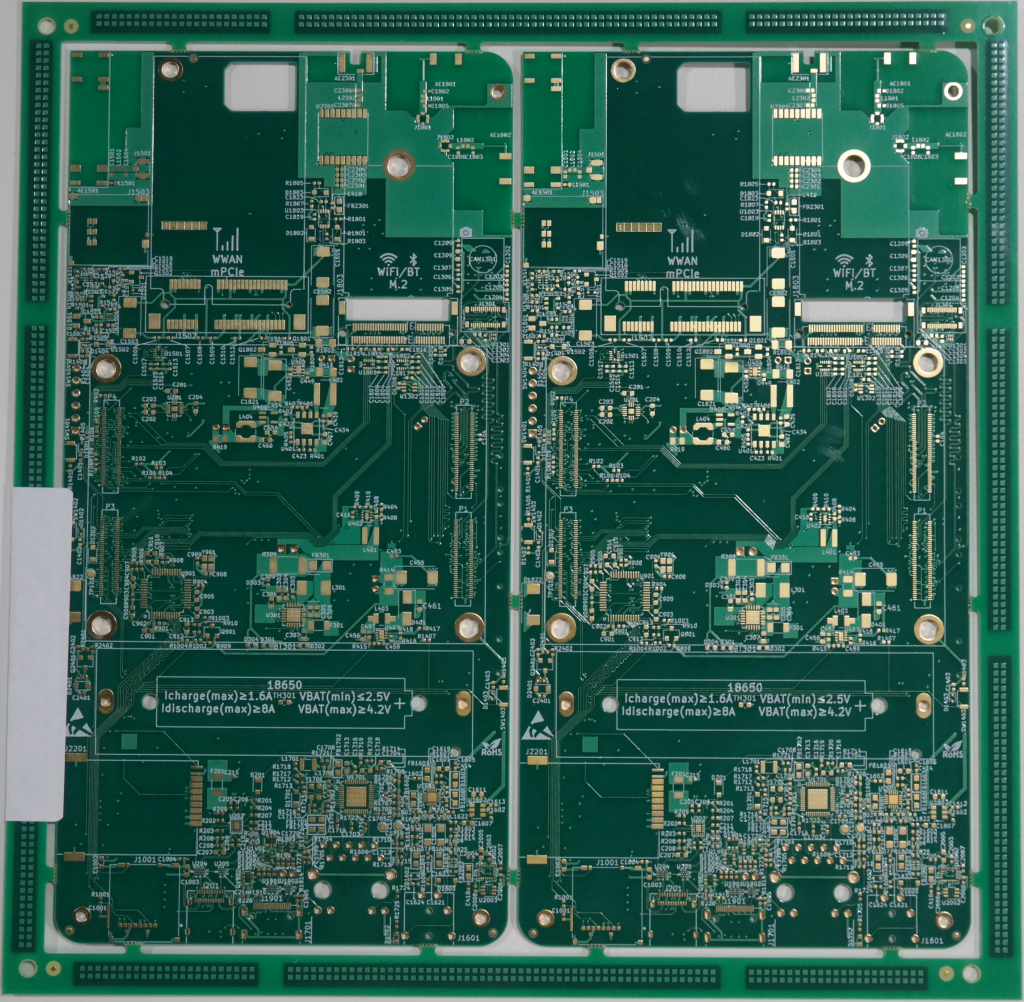 Figure 14: Prototype v0.1.2 dev kit panel (before assembly)
After the small batch of prototypes were assembled they were quickly shipped to team members for debugging and software development. Luckily, due to constant review of the design from several parties as well as persistent scrutinization, there were very few errors found in the prototype’s hardware design (three relatively minor layout/netlist adjustments and one mechanical fix). For the following two months the prototypes were used to help bring the software to a more polished state.
Final Production and Shipping
At around early-to-mid November, after making the minor adjustments needed to the hardware design, and once we were at a comfortable state where nearly every hardware subsystem was validated, we went through the process of re-exporting and delivering the manufacturing files to our hand-picked fabrication and assembly house for the final build. At this point, a few of us at Purism used December 10th-22nd as a dedicated time to help with the assembly, testing, packing, and shipping of the final units which went out to backers (many of which were delivered before Christmas!).
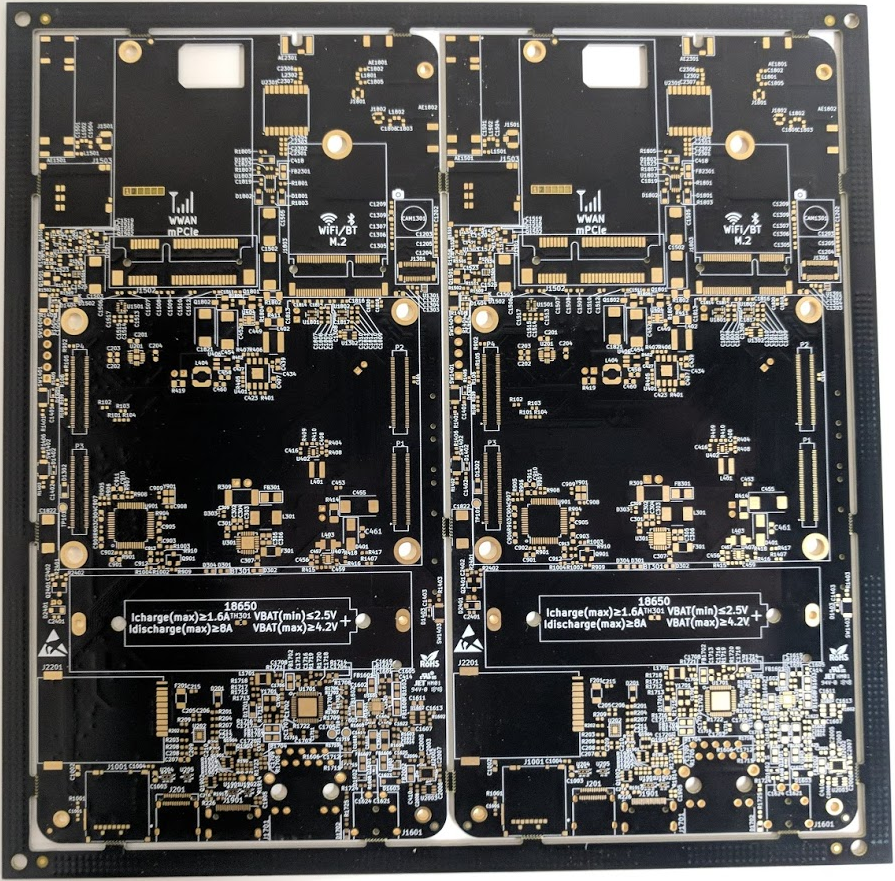 Figure 15: Final v1.0.0 dev kit panel (before assembly)
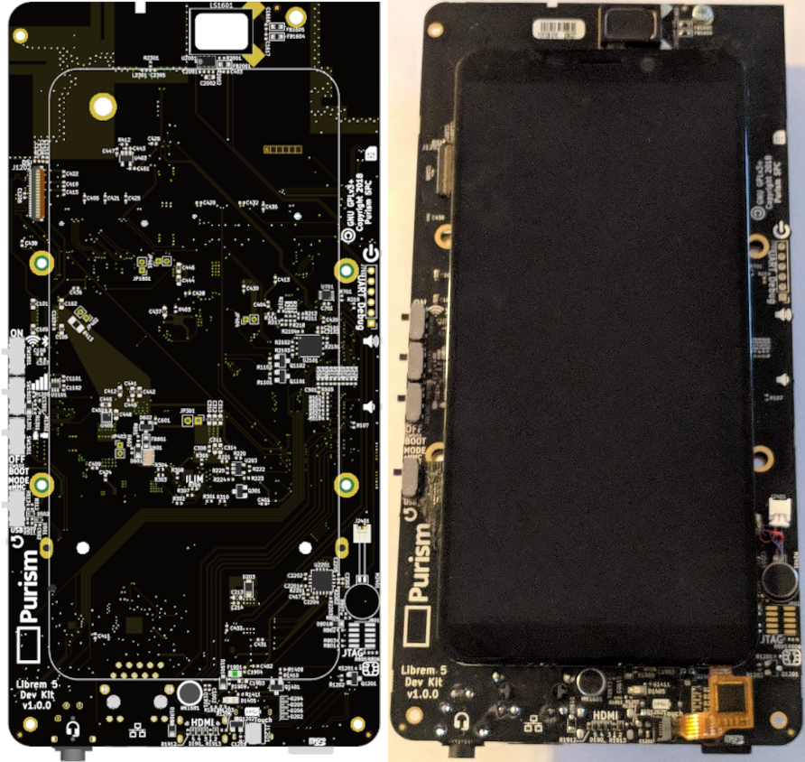
Figure 16: Fully assembled dev kit compared to the 3D view (display side)
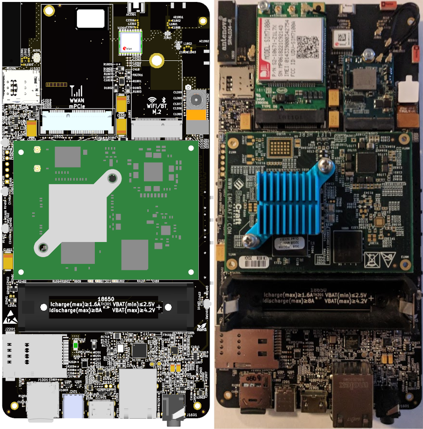
Figure 17: Fully assembled dev kit compared to the 3D view (SOM side)
The entire process was quite an intense time crunch but it was well worth it, especially after we see what the community is able to produce with our efforts. Some have even already begun designing 3D printed cases for the dev kit. We look forward to seeing what cool software and uses you come up with for these awesome boards!
After the dev kits shipped our efforts shifted toward getting the Librem 5 phone out the door. So until next time, stay inventive!
The original blog post published by Purism under CC-BY-SA 4.0 can be found here: https://puri.sm/posts/how-we-designed-the-librem-5-dev-kit-with-100-free-software/
The original publication is also archived here: https://web.archive.org/web/20191016201431/https://puri.sm/posts/how-we-designed-the-librem-5-dev-kit-with-100-free-software/
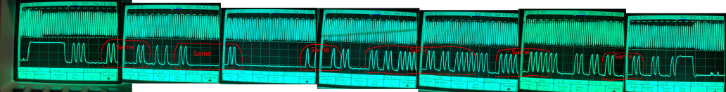
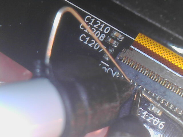
As a bonus, here’s a photo of when I scoped the MIPI DSI (CK_N and D0_P) and to try to get to the bottom of an issue we were experiencing early on (since solved):
And here’s the capture showing part of the display’s initialization while the MIPI DSI is operating in its so-called low power mode: